Logic Probe
A recent post on hackaday.com caused me to revisit my similar logic probe that I built back in university in about 1973-ish.
Noteworthy bits in the schematic:
- Input stage is a 1489 RS232 receiver, so input will accept +/- 25 volts. The bad news is that it won't work reliably with 3.3v logic, as pointed out by Hackaday commenter [doppler].
- The two 7400 gates outputs are wired together in the stupidest or gate ever. This works fine, as the low going spike from one gate can easily overpower the high output of the other gate, and the spike only lasts one gate delay.
- Rather than using capacitive coupling as in the hackaday referenced design, I use the gate delay in a 1489 to present two different inputs to the 7400 gate. This produces a low going spike on the 7400 gate output, sufficient to trigger the 555 timer.
- Vcc input protection using small signal diode (1N4148) and 6.8 ohm resistor causes small drop in input voltage to the circuit, which appears not to affect it in the slightest. It prevents the ham handed experimenter from accidentally blowing up the probe by hooking up the power leads reversed.
Click pictures to embiggen.
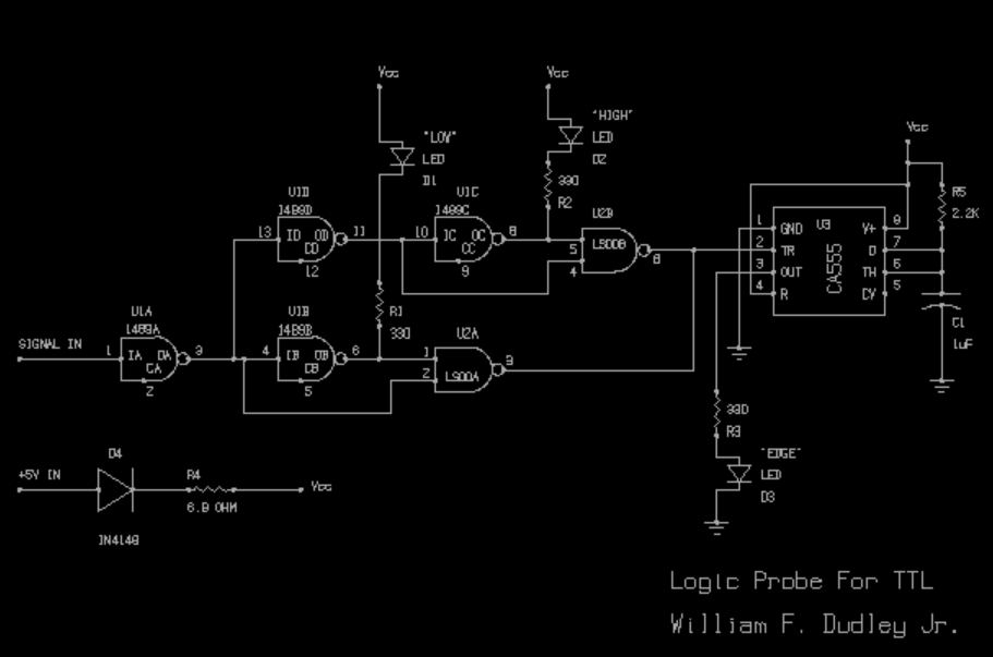
Schematic (drawn with late 80's CAD program Draftsman-EE)
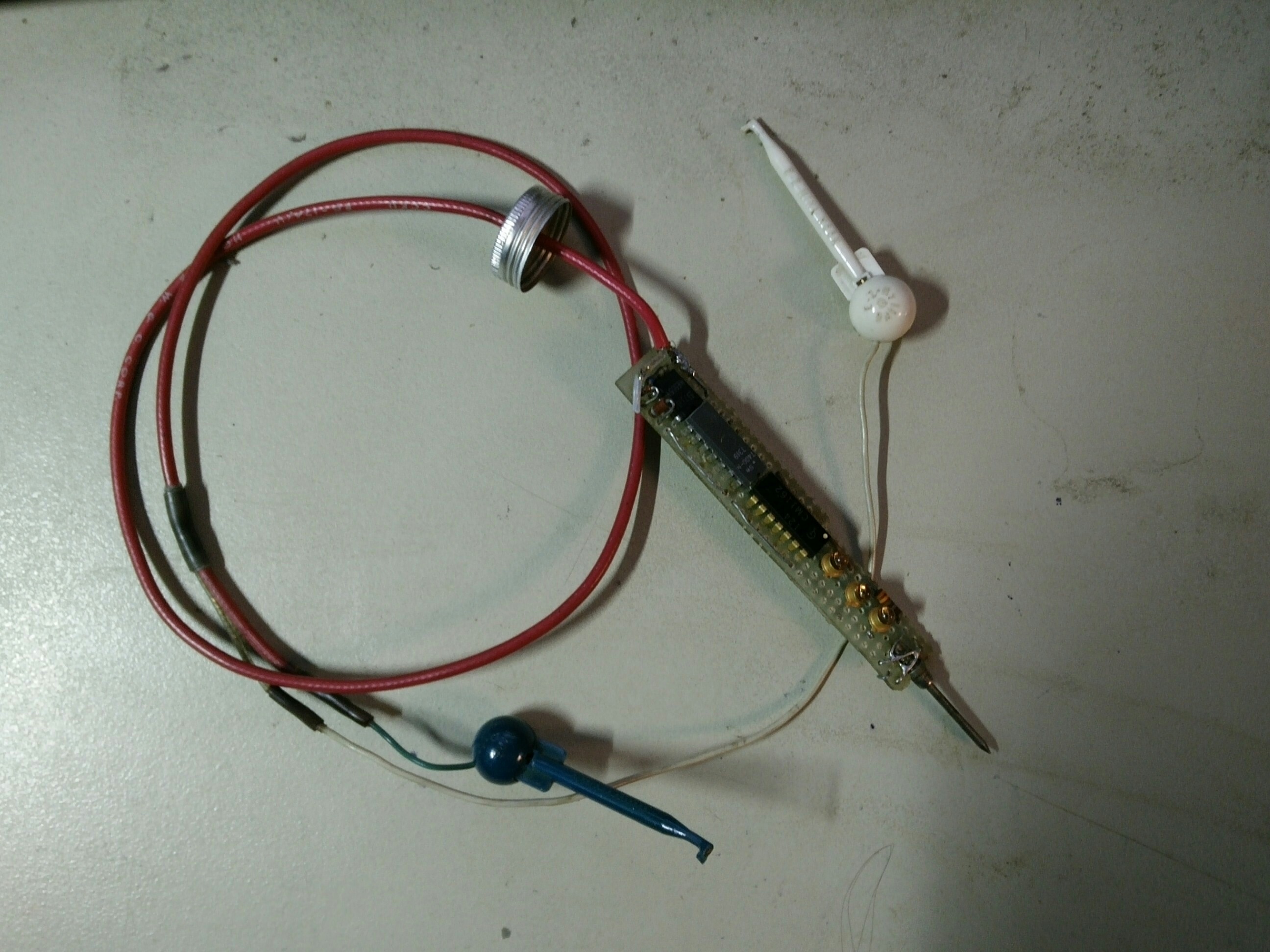
The unit out of its case. You can tell this thing is old; just look at the LEDs.
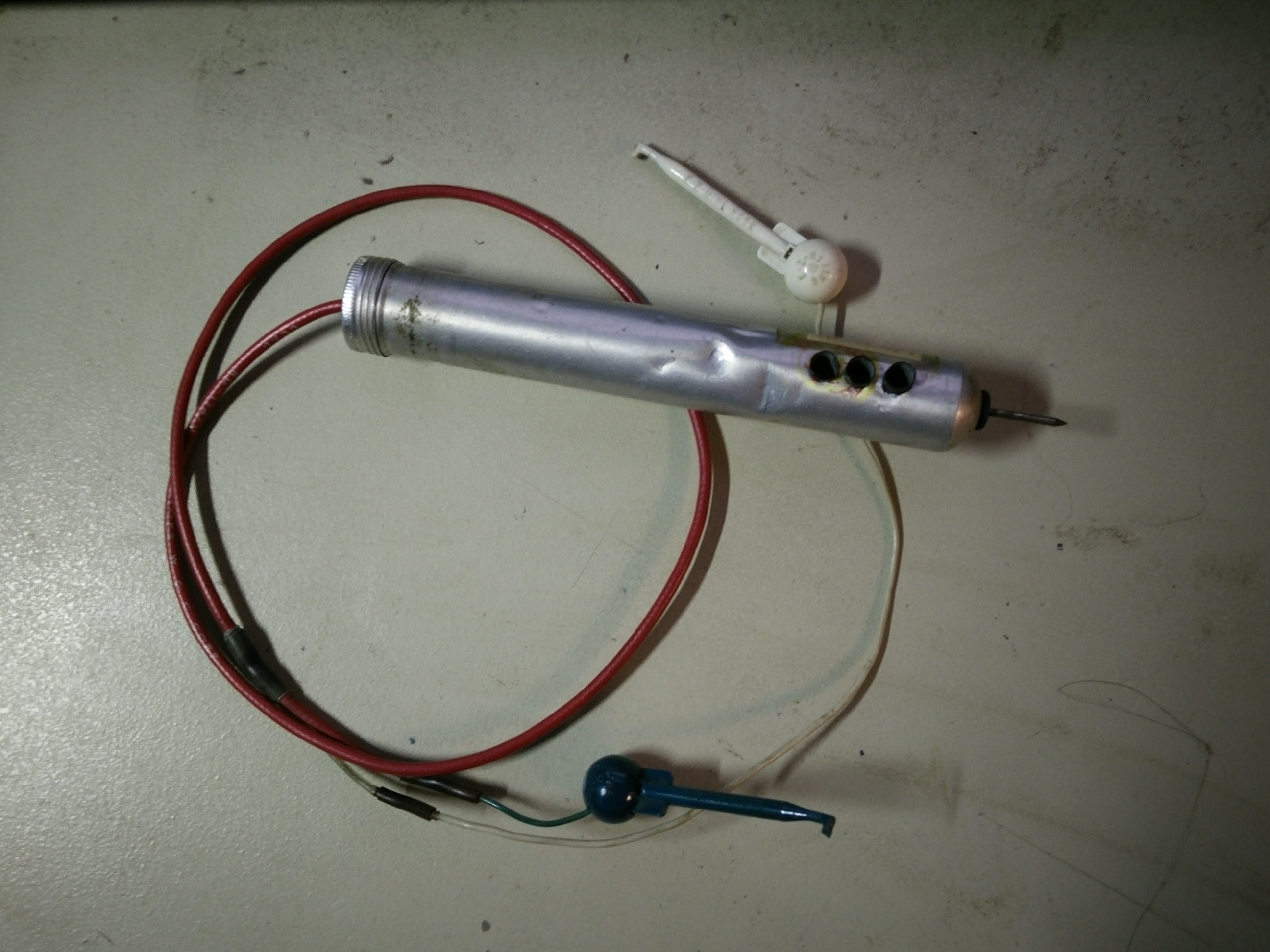
The finished unit in its cigar tube case. Note bits of heat shrink used to isolate the light outputs from the LEDs.
William Dudley
December 24, 2016


 Views
Views